Senior Process Development Engineer
This is a {Advertised Permanent / Temporary}, {Advertised Full Time / Part Time} vacancy that will close in {x} days at {xx:xx} BST.
The Vacancy
About the Role
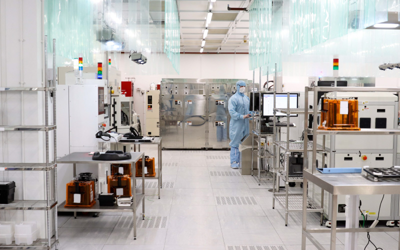
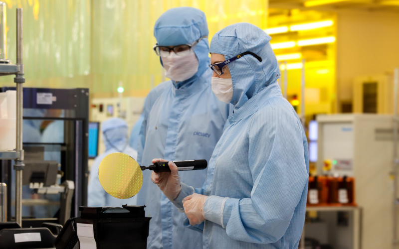
Join a fast-growing Process Development team pushing the boundaries of innovation in MicroLED and Optical Computing. Around 60% of your time will be spent in a state-of-the-art cleanroom advancing process development, and the other 40% on planning, analysing data, and presenting insights to management.
Key Responsibilities
-
You will work on all stages of process development, defining process architecture, developing process modules, working with process development tool owners to develop and optimise pixel performance.
-
Constantly seek out and implement opportunities for innovation and improvement in the products and processes
-
Participate in risk assessments and design reviews
-
Identify the requirements for new tooling to support the MicroLED and Optical Compute development roadmap, including defining process recipe specifications and aligning with the process tool owner
-
Leverage your R&D and process development experience to drive progress within a high-performing, results-oriented team
Experience & Attributes
-
A PhD degree in either of Physics, Electrical/Electronic Engineering, Material science or any relevant subject covering the field of III-V semiconductor devices
-
Hands on experience of developing and optimizing III- V, ideally III – N, semiconductor device fabrication processes in a clean room environment
-
Knowledge of semiconductor device physics
-
Broad experience in semiconductor process techniques, including but not limited to lithography (stepper and mask aligner), etch (RIE, ICP and wet etch), CVD, PVD, Evaporation, ALD, IBD
-
Design of Experiments and statistical analysis techniques
-
Understanding of LED and or Optical performance matrix and its measurement techniques such as IV response, Electroluminescence, EQE will be advantageous
-
Working knowledge of CAM systems and SPC
-
Ability to communicate clearly, design decisions to cross-functional teams
-
Experience of risk analysis and design review processes
Advantage
-
Experience with JMP or Python for data analysis
-
Experience with MicroLED or Photonics and/or optical compute technologies
-
Industry experience within Process Development
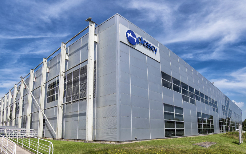
The Company
Plessey is working with world leaders in consumer technology, who are paving the way with innovative next-generation Augmented Reality and wearable applications, based on advanced microLED display solutions.
Challenging existing display technologies, microLEDs are propelling forward a vast, yet stagnated market, changing the way we interact with our devices, both for information and entertainment.
Drawing on over a decade of semiconductor and optoelectronics expertise, Plessey has developed an award-winning, unique, and proprietary GaN-on-Silicon platform and monolithic process at its state-of-the-art manufacturing facility.
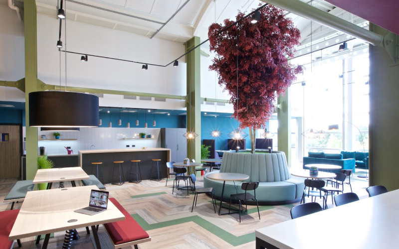
Life at Plessey
For more information, visit www.plesseysemiconductors.com/careers.
The Benefits
Cycle to work scheme
Group personal pension plan and life assurance
28 days holiday plus bank holidays
Subsidised gym and subsidised canteen
Private health and dental schemes
Free on-site parking
Discretionary Bonus Scheme
Employee Assistance Programme
Free fruit and hot drinks
Employee referral scheme
Technology & innovation awards programme
Staff
events
Testimonials
Jacquiline, Principal Process Engineer
Ross, Device Engineer
Documents
Alternatively, please sign in with...
Published
Not PublishedClosing
in X days